OnSpec xSil 257 – Hi-Speed USB to CE-ATA, Serial Media R/W Controller
Description
OnSpec’s xSil 257 Controller for Industry standard flash memories with serial interface and open standards like SD and SD HC etc is a USB to Media Multi-Slot controller. This device is ideal for Multi-Slot applications for media with serial interfaces. It also takes advantage of the new media types with faster transfer rates and higher memory capacities. It is a complete System-On-Chip (SOC) solution for interfacing various flash media to Full Speed USB (USB 1.1) or Hi-Speed USB (USB 2.0) Bus.
OnSpec offers reference designs, firmware, drivers, and manufacturing test software to make product development easy. OnSpec’s patented technology provides optimum throughput and superior flash media compatibility.
Features
-
Supports Industry standard flash memories with serial interface and open standards like SD and SD HC etc (total of 27 media formats).
-
Compatible with Microsoft Windows XP, Windows Me, Windows 2000, Windows 98, Windows 95b, Apple OS X and Linux Kernel V2.4 or later
-
Windows 2000, Windows 98/ 98SE/ 95b and Apple OS8.6 and OS9 Multi-LUN Mass Storage Class Drivers Available
-
Multiple Icons supported in Windows and Mac
-
Single and Multiple Connector Support
-
Single chip with integrated USB 2.0 PHY
-
Serial EEPROM support for sizes 256bits to 512KBits
-
Supports up 2 slots, and 2 icons at a time. (Application notes available.)
-
Supports CE-ATA
BlockDiagram
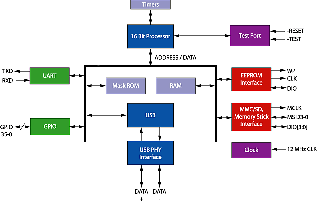
Functional Description
The xSil 257 is designed to connect serial interface media to USB. It features the following:
-
48-pin 7mm x 7mm QFP package
-
Single chip with integrated USB 2.0 PHY
-
Serial EEPROM port
-
115K Baud Serial port
-
Two General Purpose Timers
-
Watchdog Timer
-
16 bit Processor
-
Programmable Read and Write widths
-
Optimum hardware controlled transfer for speed and scalability
Packaging
The xSil 257 is a 48 pin QFP package.
USB Engine
The xSil 257 meets the Universal Serial Bus (USB) specification V2.0 and V1.1.
Serial EEPROM Port
The xSil 257 provides a serial interface to access external EEPROM’s. The interface is implemented using General Purpose I/O signals and can support a variety of serial EEPROM formats.
Serial port
Supports 7200 to 115.2K baud. Is useful as a debug port and can also be used to access the EEPROM for Reads / Writes from the serial port.
General Purpose Timers
Two general-purpose timers, Timer0 and Timer1 are provided to allow firmware programmers to keep track of timeouts as well as to generate delays.
Watchdog Timer
A Watchdog Timer (WT) is provided to enable catastrophic events to interrupt the processor. The Watchdog Timer overflow causes an internal processor reset. The Processor can read the WT bit after exiting reset to determine if the WT bit is set. If it is set, a watchdog timeout occurred. The timeout is selectable to any of the following values: 1 second, 4 seconds, 8 seconds or 16 seconds.
xSil 257 Processor
The xSil 257 Processor has a built-in 16-bit processor along with a BIOS ROM. The processor operates with a specialized instruction set optimized for Mass Storage applications and USB transaction processing. The start up code for the 16-bit processor resides in a masked ROM.
RAM Interface
The xSil 257 chip comes with an Internal RAM. Data is transferred in EHS (Extra High Speed) mode to ensure optimum transfer speeds.
Masked ROM
The Masked ROM consists of the xSil 257 processor start-up code and the functions listed below:
-
Power On Initialization
-
USB packet transaction management
-
USB Power Management (S0..S3 modes)
-
USB Enumeration Management
-
API support for USB transactions, EEPROM Interface, Memory Management etc.
The firmware is easily extended / expanded by using External Serial EEPROM. The BIOS provides several services to facilitate this expansion code. At boot-up time, the scan services of the BIOS search for the expansion signature in the Serial EEPROM as well as via the UART and USB. For more information, refer to Applications section of this manual.
The BIOS API functions are designed as Software Interrupts, making it easy for enhancements. Any Interrupt can be enhanced / modified by inserting the user defined function in the interrupt placeholder. When this interrupt is called by the BIOS, the user defined function is called first to enhance the behavior before passing it on to the standard BIOS function’s call or return without passing it on.
Programmable Read and Write cycles
The external cycles to flash using the D[15:0], and SM[7:0] buses are software configurable
Ordering Information
|
Part Number |
Description |
Packaging |
|
xSil 257 |
USB 2.0 standard flash memories with serial interface and open standards like SD and SD HC etc Read/ Write Controller. |
48 LQFP Lead Free (RoHS Compliant)
|
Technical and Design-in Information
Contact: sales@siliconapps.com
Design Support (Will be provided by OnSpec upon request)
-
Card Manufacturer Compatibility Testing (Software Release Notes)
-
Read/Write Performance Testing (Software Release Notes)
-
USB IF Certification Lab Report Summary
-
IBIS Models (Available on request)
-
Qualification Report
-
BIOS Boot Over USB Compatibility Testing Report
-
Flash Media Association Contact List
-
Memory Stick and xD Picture Card Certification and Lab Test Results
-
Card Reader Device Comparison
-
Embedded OS Compatibility Testing with XXXXXX MSC Driver
-
Reference board layout details click here to contact sales@siliconapps.com
Available from OnSpec under Software License Agreement (SLA):
Click Wrap SLA Agreement for Object Code on OnSpec Website
Manufacturing Utilities
Firmware up gradation through flash media
Software Release Notes (Important for Attribute Bit Settings and Descriptions)
Software Test Report (Matrix of OS and PC Chipset Testing)
Windows 98 and 2000 Multi-LUN Drivers
Vendor Specific Command Support Specifications with Source Code License
Email Notification of New Firmware Object Code Downloadable Over the OnSpec Secure Website
Patents:
OnSpecLink® Family of Products
This product is covered by one or more of the following patents:
US Pat. 5841424, 6438638, 6832281, 6859361, 6859369
Taiwan Pat. I 222564
Other Foreign & US Patents Pending
Memory Stick Compliant Products Test Specification Extract Version1.1.00:
Certified, Reference: 20050401 (First controller in the world to get this certification)
Disclaimer:
Information in this document is provided in connection with OnSpec Electronic products. No license, express or implied, by estoppels or otherwise, to any intellectual property rights is granted by this document. Except as provided in OnSpec Electronic’s Terms and Conditions of Sale for such products, OnSpec Electronic assumes no liability whatsoever, and OnSpec Electronic disclaims any express or implied warranty, relating to sale and/or use of OnSpec Electronic products including liability or warranties relating to fitness for a particular purpose, merchantability, or infringement or any patent, copyright or other intellectual property right.
OnSpec Electronic products are not intended for use in medical, life saving, or life sustaining applications.
Trademarks:
OnSpecLink Is a registered trademark of OnSpec Electronic, Inc.
All trademarks are the properties of their respective owners.
Download: Product Sheet PDF Size=64KB